Original Link: https://www.anandtech.com/show/359
VIA Apollo Pro 133: A Camino Preview
by Anand Lal Shimpi on August 16, 1999 6:03 AM EST- Posted in
- Motherboards
There are two types of successful people, those that climb their way to the top and slow down once they reach there, and those that never stop climbing. Intel has been enjoying the fruits of success for the past few years by being a company that climbed their way to the top with the power and finesse that we've come to expect from Intel. Unfortunately, after turning around to see the competition nowhere near the mountain Intel had just climbed, the company then began to slow down and thus gave room for a number of companies to step in and obtain some of the territory Intel had spent years on gaining and securing.
On the desktop microprocessor side of the mountain, AMD, with the recent release of their Athlon processor, has taken the lead over Intel in terms of producing a more advanced, architecturally, processor. And more relevant to the topic at hand, VIA Technologies is attempting to jump the gun on Intel's release of their Camino (820) chipset with the first Slot-1/Socket-370 chipset with official support for the 133MHz Front Side Bus (FSB), the Apollo Pro 133.
Attempt #1
VIA's first real attempt at going head to head with Intel in the Slot-1 arena was with the Apollo Pro chipset. The Apollo Pro chipset was actually announced during the days of the Pentium Pro as the first non-Intel Socket-8 chipset, however the first time the chipset really made it into the eyes of the public was at Fall Comdex '98.
The situation was quite funny actually, at the time VIA was engaged in a court battle with Intel over the rights to manufacturer a chipset that supported the Pentium II's GTL+ bus. Because of the legal entanglements, VIA couldn't advertise their own Slot-1/Socket-370 chipset solution at Comdex, so in VIA's massive booth at Comdex in the Pentium II motherboard display all references to the VIA chipset in the specs of the motherboards displayed were covered up by a piece of tape just prior to the opening day of Comdex. Just a couple days later, VIA re-announced the Apollo Pro chipset after obtaining the legal rights to do so under the name Apollo Pro Plus. The Apollo Pro Plus, albeit a separate chipset (VT82C693) was essentially the Apollo Pro chipset with official support for Socket-370 platforms as well as Slot-1 platforms.
By this time, the Apollo Pro had made its way into the hands of some reviewers and had already proved itself much better at dealing with newer AGP cards than its Super7 counterpart, the MVP3. The Apollo Pro Plus was no different, the chipset featured the same compatibility list as the Intel BX but from the end user's perspective, full compatibility was an unspoken expectation. You don't normally find yourself purchasing a BX board and wondering whether or not it's going to work with your TNT2, and for the same reason VIA wanted to make sure that the end user could not tell the difference between the Apollo Pro Plus and the Intel BX, at least in a negative connotation.
Failure #1
The Apollo Pro Plus was far from a blazing success, it did the job VIA said it would but it did little more beyond that. In order for the Apollo Pro plus to be an outstanding success it would have to offer something above and beyond what Intel already offered with the BX chipset, that had already been given over 6 months of "testing" time in the hands of thousands of users by the time VIA started shipping the Apollo Pro Plus. The only real feature VIA could boast about was the ability to run the memory bus synchronously with the FSB or synchronously with the AGP bus, meaning at an unoverclocked state you could run the memory bus at 100MHz with the FSB, or at 66MHz with the AGP bus while the FSB remained at 100MHz.
In theory this would allow users to keep their old PC66 SDRAM while taking advantage of newer 100MHz FSB Pentium II processors, but you all know how well theories turn out in the computer hardware industry. The fact of the matter ended up being that most motherboard manufacturers didn't bother implementing a method of controlling the memory clock, so in essence, the Apollo Pro Plus was everything the Intel BX chipset was.
If we had left it at that, there would be no point in going after an Apollo Pro Plus based motherboard or a BX based board, as the two chipsets would essentially be the same, unfortunately that wasn't the case. There were two limiting factors that kept the Apollo Pro Plus from living up to the "glory" of the Intel BX chipset, memory timings, and AGP performance.
The memory timing issue came from the Apollo Pro Plus' SDRAM timings for back to back accesses, and has unfortunately kept the Apollo Pro back in terms of overall performance in many tests, including Business Winstone, often times a key comparison factor among motherboards that "look" the same. The performance issues didn't stop there, the AGP miniport driver and AGP implementation on the Apollo Pro Plus was noticeably slower than on an identically configured Intel BX system across the board in games. This soured many gamers on the topic of an Apollo Pro Plus based motherboard.
Of course the argument of price came up more than once in the whole VIA vs Intel debate, however the end result ended up being that BX boards were generally priced virtually identically to their "low-cost" Apollo Pro Plus based counterparts. At the same time, the Apollo Pro Plus boards never boasted the same level of features and options as the BX boards did. Case in point would be the lack of any Apollo Pro Plus based boards with on-board SCSI or RAID Port for high end systems. Who was at fault for the lack of success of the Apollo Pro Plus? The chipset itself wasn't horrible, but the lack of support from most motherboard manufacturers kept the public from widely accepting the Intel alternative.
The Apollo Pro Plus did make a healthy alternative to Intel's "low-cost" ZX and EX boards, especially on Socket-370 motherboards, however the two performance issues briefly discussed above still kept the "attractive" rating of the chipset low in the eyes of gamers and performance tweakers.
Keeping an eye on Camino
The Intel 820 chipset has become the butt of many jokes among quite a few industry analysts, motherboard manufacturers, and even your average hardware enthusiasts. The reason behind all the snickering is because Intel was adamant about pushing Rambus DRAM as a requirement for the 820 chipset, which in itself seems like a positive move for the industry. RDRAM is a more advanced memory technology and does offer more memory bandwidth than any memory technology available for the desktop market today. But, after the motherboard manufacturers got a chance to take a look at RDRAM and the 820 and realized that the cost of investment was definitely not worth the end product, they began hoping for another solution.
Motherboard manufacturers continued to manufacture new revisions of BX based motherboards, and the life of the BX chipset extended even further than the original expectations were. From the end user's perspective this isn't necessarily a bad thing, as it translates into you not having to go out and buy a new motherboard every 6 months to keep up just like with the graphics card industry. From the perspective of Intel it isn't necessarily a good thing, as it translates into the possibility for another manufacturer to step up to the challenge and release something more advanced, before Intel can even get Camino out the door.
A common misunderstanding with Camino is that it will support RDRAM only, which is, at least according to Intel, not the case. We had the benefit of talking to a few key representatives at Intel that were dealing directly with the progress on Camino and from their point of view, they are not forcing users to dive into Rambus at all. The 820 (Camino) chipset supports both RDRAM and SDRAM by default, it is up to the motherboard manufacturer to decide whether or not to support "older" SDRAM with their motherboards. The situation will most likely end up being very similar to the debates surrounding the SDRAM requirements of the 440LX chipset back in 1997. The LX chipset supported both EDO and SDRAM, however Intel was strongly pushing SDRAM and the result ended up being that very few motherboard manufacturers produced a LX motherboard with support for EDO RAM although the chipset clearly supported the memory technology.
Intel is considering support for PC133 on Camino, and it wouldn't be surprising at all if we saw Camino motherboards pop up with PC133 support with an eventual transition to Rambus as the yields on such products improve.
Enter the VIA Apollo Pro 133
Now we have VIA's alternative solution, if you recall, we just compared the Intel BX chipset to the VIA Apollo Pro and came away with the conclusion that, outside of performance, there was very little that set the two apart. Most motherboard manufacturers like the idea of having a pin compatible chipset that would essentially "plug-in" to their current designs, thus eliminating the need to redesign for new chipsets and new memory designs, while adding support for the 133MHz FSB and AGP 4X. This is what VIA is planning on accomplishing with the Apollo Pro 133.
The Apollo Pro 133 is the same 2 chip solution that made up the Apollo Pro and the Apollo Pro Plus, with two major changes, the official support for the 133MHz FSB, and the future support for AGP 4X. Take away Rambus and doesn't this sound a lot like Intel's Camino chipset? Let's dig deeper...
North/South Bridge vs Accelerated Hub Architecture
Since the dawn of the single chip solution, the idea of creating chipset solutions with interchangeable "parts" was the goal in order to keep flexibility at a maximum. The theory was then translated into what is now known as the North/South bridge architecture, where the main memory/graphics controller is housed in a chip that makes up the North bridge and all I/O functions are handled in a chip known as the South bridge. In theory, a single North bridge could be coupled with one of three different south bridges in order to tailor to the needs of various types of computer users. In practice, no chipset manufacturer has truly used this technology to its full potential.
VIA has started to do so with their two most popular south bridges, the Mobile South Bridge (VT82C596A) or the Super South Bridge (VT82C686A) controller. The main difference between the two south bridges is that the Super South Bridge offers support for AMR (Audio Modem Riser - see Intel 810 Review) as well as Ultra ATA 66, a feature currently only supported in one of Intel's chipsets, the 810 and due for support in the 820 (Camino). The beauty behind this design is that it doesn't cost motherboard manufacturers very much to implement the Super South Bridge in their designs that already feature the Mobile South Bridge. As soon as VIA ramps up production on the Super South Bridge parts, the motherboard manufacturers can then use the new south bridge in their designs and sell all of their boards that feature the older south bridge at a lower cost while offering the boards equipped with the newer south bridge at an increased cost.
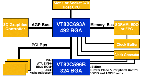
But why stop there? In theory (don't you love those two words?), if the demand were high enough, VIA's Firewire controller could be integrated into the south bridge design and motherboard manufacturers would then have the option of selling a third type of Apollo Pro 133 based motherboard with integrated Firewire. Or, if the demand for on-board Ethernet were great enough, VIA could integrate Ethernet functionality into the south bridge thus increasing the number of options users would have when going after a motherboard based on a VIA chipset. The possibilities are endless, and moving the chipset design to a 0.18 micron fabrication process just increases the amount of room VIA will have to work with. But why doesn't VIA just go ahead and do it? As alluded to above, the demand just isn't there, for a manufacturer to make such a move they would have to weigh out the costs of implementation vs the resulting increase in sales, and currently, the numbers just aren't working. VIA is definitely aware of the potential, as quite a few of their representatives were preaching to the crowd about the possibilities at last year's Fall Comdex, it's just a matter of time before it happens.
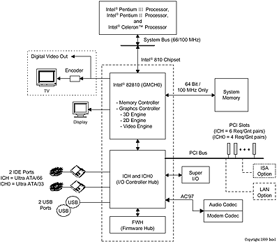
Intel is taking a different approach to chipset manufacturing after years of dealing with the same old North/South bridge combination, they recently debuted their Accelerated Hub Architecture (AHA) with the 810 chipset. Instead of having everything communicate with the memory/CPU via the PCI bus, the new Accelerated Hub Architecture allows for direct communication between the memory/CPU and disks, peripherals, and in the case of the i810 chipset, the graphics adapter.
The key to the success of the Accelerated Hub Architecture is the substitution of individual hub interfaces for the PCI bus in connecting the various parts of your system to your memory/CPU on the motherboard end of things. Take a look at the acronym PCI, Peripheral Component Interconnect, it doesn't really scream "all-purpose-bus" now does it? Intel took what was once a two-chip solution (North/South Bridge) and converted it into a two chip, three-hub solution, the first implementation being the i810 chipset. The three individual hubs are the Graphics and Memory Controller Hub (GMCH), the I/O Controller Hub (ICH) and the Firmware Hub (FWH). The two main hubs, the GMCH and the ICH are connected via an internal bus that offers double the bandwidth of the PCI bus, 266MB/s. This is a definite improvement over the "old" way of doing things and will shortly become the new standard as far as chipsets go, don't expect Intel to return to the classical way of doing things on the motherboard level anytime soon.
It wouldn't be surprising to see VIA adopt an approach similar to Intel's AHA, but such a move wouldn't occur until much further down the line in the development of VIA chipsets. In any case, a key difference between the Apollo Pro 133 and the soon to come i820 is the architecture behind the two chipsets, the conventional North/South bridge setup vs Intel's Accelerated Hub Architecture.
What about overclocking?
Although most newer BX motherboards already support FSB frequencies of 133MHz and above, the problem with overclocking the FSB past 100MHz on current BX and Apollo Pro Plus motherboards is the frequency it places the rest of your system at. The problem with the North/South bridge architecture of most of our chipsets is that most of the operating frequencies are dependent upon one another. For example, if you overclock your FSB to 133MHz (on a 100MHz BX board) your PCI bus that was once running at 100MHz/3 is now running at 133MHz/3. Granted that most newer boards now support the 1/4 PCI clock divider which would put your PCI bus at 133MHz/4, but what about your AGP card?
The current AGP 2X specification calls for a 66MHz clock frequency of all AGP cards, unfortunately the AGP frequency is determined by multiplying your FSB by a certain fraction. In the case of the BX and Apollo Pro Plus chipsets, the only fractions available are 1/1 and 2/3. With the 66MHz FSB, the 1/1 ratio is used as this would keep the AGP frequency at 66MHz or at a 1-to-1 ratio with the FSB. With the 100MHz FSB, the 2/3 ratio is used as this keeps the AGP frequency at 66MHz, or at 2/3 of the FSB. But what happens if you overclock to 133MHz? If you multiply 133MHz by 2/3, you get approximately 89MHz, or a clock frequency 33% over the AGP 2X specification.
The truth of the matter is that there isn't a single 3D AGP accelerator on the market today that can work reliably at 89MHz in mass quantities. Even the most reliable cards have some difficulty working at the 83MHz frequency they are forced to work at if your FSB is running at 124MHz. This puts overclocking your current BX platform to 133MHz an almost impossible task to accomplish if you still plan on using your system for more than showing off your overclocked creation.
What's New about the Apollo Pro 133
The Apollo Pro 133 fixes the "problems" that kept most of us from overclocking to the 133MHz FSB on our BX and Apollo Pro Plus motherboards. By adding support for the 1/2 AGP clock divider, the chipset now allows for much greater FSB frequencies such as 133MHz and even higher overclocked frequencies as your AGP clock will be running at 1/2 the FSB. In the case of the 133MHz FSB, this leaves your AGP clock running at a comfortable 66MHz.
At a 133MHz FSB, all your PCI devices operate at 1/4 the FSB, or 33MHz, which is exactly what the PCI 2.2 specification calls for. This includes your on-board EIDE controller as it is tied into the PCI bus, so you don't have to worry about your hard drives crapping out when you use the officially supported 133MHz FSB frequency.
As mentioned before, when using the Super South Bridge controller, a decision left entirely up to the motherboard manufacturer, the Apollo Pro 133 can extend its support to include Ultra ATA 66 devices as well as AMR devices. Keep in mind that this support won't go without an added cost, however the increase in price should be minimal.
The 1/2 AGP clock divider opens up a word of new possibilities for overclocking. The 133MHz+ FSB settings are now much more viable options, even at 150MHz, the AGP bus is still running at 75MHz which is around 14% over the specification, and is manageable for most AGP cards (it's almost the equivalent of running the 112MHz FSB on a BX board). At 150MHz, your PCI bus will be running at 37.5MHz, or 1/4 of 150MHz, which is also very manageable for most PCI cards as it is the equivalent of running your FSB at 75MHz on a motherboard that only supports the 1/2 PCI clock divider. Unfortunately with all Intel CPUs shipping in clock locked states, putting the 133MHz+ FSB settings to use would be overclocking your CPU far beyond reasonable limits, so you're most likely going to have to wait until 133MHz FSB CPUs begin shipping before taking the full advantage of any chipsets with 133MHz FSB support. And since Intel controls the flow of CPUs in to the market, the first 133MHz CPUs will hit conveniently with the launch of the Intel Camino chipset, but the same overclocking principles apply to the Camino as well.
The only limiting factor with overclocking your FSB on a chipset with official 133MHz support would be keeping your memory at a reasonable frequency. Luckily, the Apollo Pro 133 allows you to run your memory bus at three frequencies, your FSB clock, your FSB clock + 33MHz, or your FSB clock - 33MHz. This means that with your FSB at 133MHz, your memory can either be operating at 133MHz, 100MHz, or 166MHz but most motherboard manufacturers will disable the ability to run your memory bus at speeds greater than 133MHz. So in the case of the 150MHz overclocked FSB frequency, you could keep your memory bus at a manageable 117MHz, a setting most high quality PC100 SDRAM will do just fine.
The Camino chipset will have a different approach to the memory frequency. If a motherboard manufacturer does decide to include PC133 support on their Camino based motherboard, the memory bus will operate asynchonously at 133MHz, regardless of your FSB setting. This approach is much like how the 810 chipset keeps your memory bus at 100MHz, regardless of your FSB frequency, even if your FSB is clocked at a slower 66MHz which happens to be the case with all current un-overclocked Socket-370 810 boards.
The memory timing issues that originally plagued the Apollo Pro Plus have since been fixed with the Apollo Pro 133, so the memory performance of the Apollo Pro 133 should be much improved over its predecessor and it should be much closer to the level of the Intel BX chipset. But we'll leave all performance discussions to the benchmarks which are coming up next...
The First 133MHz FSB CPUs
Since all Intel CPUs are now clock locked you can't simply lower the clock multiplier and use the 133MHz FSB to gain the performance boost, so the true users of the FSB frequency will start popping up with the release of the first 133MHz FSB CPUs.
Just like with the first 100MHz FSB CPUs, the motherboard will perform a pin state detect of a previously unused pin on the processor. In the case of the first 100MHz FSB CPUs, the pin was B21. If B21 was set to high, the CPU was a 100MHz FSB CPU and the motherboard would make sure that the FSB frequency was set to 100MHz. If B21 was set to low, the CPU was a 66MHz FSB CPU and the motherboard would make sure that the FSB frequency was set to 66MHz.
With the first 133MHz FSB CPUs a reserved pin will be used to identify the specified FSB for that processor. The pin assignment isn't known at this time but when set to high, it will indicate a 133MHz FSB CPU is present and the motherboard will then enable the 133MHz FSB. When set to low, it will indicate either a 66 or 100MHz FSB CPU and the motherboard will then detect the state of pin B21 to determine what FSB to use.
As with pin B21, it shouldn't be too difficult to "fool" motherboards that perform an auto-detect of what type of processor is installed in the system (whether it is a 66/100/133MHz FSB CPU) by either using a jumper setting on the motherboard (as was the case in our test system) or by possibly taping the pin using the B21 "trick" first introduced to the community by Tom's Hardware.
The Test
AnandTech used an Intel Pentium III 600 in all of the tests, the processor was either clocked at 100MHz x 6.0 in the case of all 100MHz FSB tests or 133MHz x 4.5 in the case of all 133MHz FSB tests.
The two VIA based motherboards were the AOpen AX63 (Apollo Pro Plus) and the AOpen AX63 Pro (Apollo Pro 133). Both used the latest BIOS updates and were configured optimally for performance using the fastest SDRAM (222) timings. |
The Intel BX based motherboard used was the ABIT BX6 Revision 2.0 and featured the latest BIOS update as of August 15, 1999 and was configured optimally for performance using the fastest SDRAM (222) timings.
Both systems used the same 128MB SDRAM module manufactured by Enhanced Memory Systems, and is guaranteed for 133MHz FSB operation.
The test hard drive was a Western Digital 8.4GB Ultra ATA 33 HDD.
The AOpen AX63 and AX63 Pro both featured the Mobile South Bridge VT82C596A. The two VIA based boards used similar North Bridge chips, the AX63 (Apollo Pro Plus) used the VT82C693 and the AX63 Pro (Apollo Pro 133) used the VT82C693A. The only difference between the two North bridge chips is that the VT82C693A officially supports the 133MHz FSB and thus supports the 1/2 AGP clock divider.
Windows 98 SE was installed on all test systems, and the latest drivers were common to all systems. The two VIA boards used the VIA Service Pack 4.01 for all driver installations.
A default clocked NVIDIA Riva TNT2 Ultra (150MHz core / 183MHz memory) was used as the common graphics cards in all tests. The TNT2 Ultra was picked due to its excellent drivers and full AGP 2X implementation to properly illustrate performance differences between all chipsets.
Business Application Performance
Chipset (Mem/FSB) |
Business Winstone 99 | Avid Cinema* | Adobe Photodeluxe 3.1* | Naturally Speaking Prof 3.52* | Netshow Encoder 3.0* | Photoshop 5.0* |
| Intel 440BX (100/100) | 26.3 | 104.6 | 96.7 | 286.8 | 163.8 | 108.2 |
| VIA Apollo Pro 133 (100/100) | 26.3 | 112.8 | 102.5 | 326 | 156.9 | 103.2 |
| VIA Apollo Pro 133 (100/133) | 26.4 | 106.1 | 99 | 312 | 152.1 | 102.8 |
| VIA Apollo Pro 133 (133/100) | 26.3 | 106.6 | 99.4 | 316.5 | 151.4 | 101.8 |
| VIA Apollo Pro 133 (133/133) | 26.4 | 104 | 96.5 | 293.4 | 147.2 | 101.1 |
| VIA Apollo Pro Plus (100/100) | 26 | 113.1 | 106.7 | 334.6 | 160.8 | 105.6 |
* Scores are Time in Seconds, lower is better

As you can see, for business applications, the 133MHz FSB gives the Apollo Pro 133 the advantage over the Intel BX. Also, the memory timings have definitely improved keeping the Apollo Pro 133 on par with the Intel BX even when using the 100MHz FSB/Memory clock.
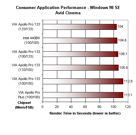
The 133MHz FSB comes in handy with streaming video and the 133MHz memory bus clock comes in handy with video editing applications that are dependent on streaming memory accesses as well, giving the Apollo Pro 133 the lead, albeit a small one, over the Intel BX.
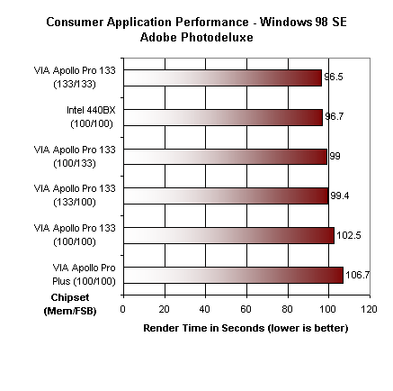
Adobe Photodeluxe, an image editing package (sort of like Photoshop lite), benefits more from a faster FSB than a faster memory bus, which keeps the Apollo Pro 133 on top, followed by the Intel BX which is not that far behind due to better overall performance. It wouldn't be surprising to see the Camino come out on top of all of the contenders here, but for actual numbers we'll just have to wait and see.
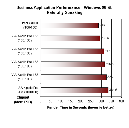
The Naturally Speaking benchmark is the first test in which the BX chipset at 100MHz FSB and 100MHz memory clock comes out on top of the Apollo Pro 133 with its 33% faster memory/FSB clocks. For those of you not familiar with the application, Naturally Speaking is a voice dictation software package and the nature of the benchmark favors the BX chipset due to a difference in memory timings between the BX and Apollo Pro 133 and Pro Plus chipsets.
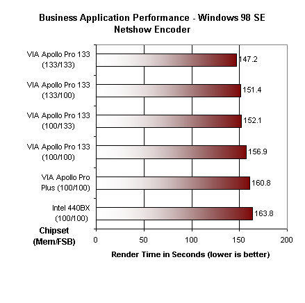
...and contrary to the previous benchmark, the last two benchmarks favor the VIA chipsets. However you must keep in mind that most of the performance differences are minimal, with the BX chipset excelling in some applications, and the VIA chipsets taking the lead in others. As a business/consumer level application solution, the Apollo Pro Plus and the Apollo Pro 133 are both excellent alternatives to the Intel BX, but how does the picture change when gamers are introduced to the chipset?

AGP Gaming Performance
Quake 3 Arena Test v1.08 q3demo1.dm3 |
|||
| Fastest | Fast | Normal | |
| Intel 440BX (100/100) | 98.5 | 91.5 | 83.2 |
| VIA Apollo Pro 133 (100/100) | 87.4 | 81.8 | 73.9 |
| VIA Apollo Pro 133 (100/133) | 89.6 | 84 | 75.5 |
| VIA Apollo Pro 133 (133/100) | 90.1 | 84.5 | 76.5 |
| VIA Apollo Pro 133 (133/133) | 90.9 | 85.3 | 77.2 |
| VIA Apollo Pro Plus (100/100) | 82.1 | 76.4 | 67.8 |
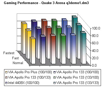
Quake 3 Arena test is noticeably slower on all VIA chipsets, regardless of FSB, when compared to the Intel BX. The performance difference is around 17% at worst using the old Apollo Pro Plus and around 8% at 133MHz FSB using the Apollo Pro 133. To the occasional gamer, the performance difference isn't great, but to the hard core gamer the drop in frame rate is unacceptable.
Even with the 133MHz FSB, the Apollo Pro 133 is not a viable option for a performance oriented gamer.
| Chipset (mem/fsb) | VIA Apollo Pro Plus (100/100) | VIA Apollo Pro 133 (133/100) | VIA Apollo Pro 133 (100/100) | VIA Apollo Pro 133 (100/133) | VIA Apollo Pro 133 (133/133) | Intel 440BX (100/100) |
| 3DMark 99 Texture Transfer Tests | ||||||
| 2MB | 73.1 | 73.1 | 73.1 | 73.1 | 77.1 | 73.2 |
| 4MB | 55.8 | 55.7 | 55.8 | 55.8 | 57.7 | 56.8 |
| 8MB | 36.2 | 36.2 | 36.2 | 36.2 | 36.7 | 37.4 |
| 16MB | 20.7 | 20.6 | 20.7 | 20.7 | 20.8 | 21.6 |
| 32MB | 1.6 | 2.0 | 2.0 | 2.1 | 2.2 | 2.6 |
| 3D Winbench Texturing Tests | ||||||
| Small | 32.3 | 32.8 | 32.8 | 32.8 | 32.8 | 33.0 |
| Medium | 15.5 | 17.1 | 16.6 | 16.6 | 17.1 | 17.3 |
| Large | 14.4 | 16.1 | 15.4 | 15.4 | 16.1 | 16.1 |
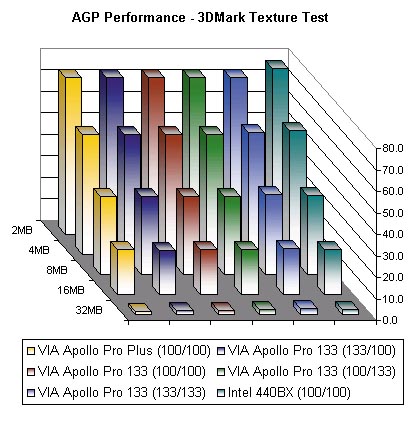
The AGP implementation on all of the VIA chipsets is also noticeably slower, strengthening the argument that for the performance oriented gamer, Intel is still probably the best solution for Slot-1/Socket-370 users. The Camino chipset should be slightly faster than the BX, but once again, for actual numbers we'll have to play the waiting game.
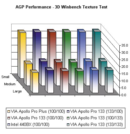
The 3D Winbench texture test is another great way of measuring AGP performance differences, and although the Apollo Pro 133 is still noticeably faster than its predecessor, the Apollo Pro Plus, the VIA AGP implementation still lacks behind the Intel BX.
Final Words
For a hardcore gamer, the Apollo Pro 133 is nothing more than a small preview of the benefits the Camino chipset will bring. But by no means is it a viable option for those gamers that are very performance oriented (as many of them seem to be). The stability of most Apollo Pro 133 boards should be on par with the average BX boards, the AX63 Pro we tested gave us generally stable operation however stability shouldn't be something you look for in a motherboard, it should be given to you without even asking.
For the average computer user, the Apollo Pro 133 offers a few advantages over the Intel BX, but until the first 133MHz FSB CPUs hit the streets, most of those advantages will remain to be seen. In business and consumer level applications, the Apollo Pro 133 will have difficultly discerning itself from the Intel BX in both a positive and a negative manner.
It seems like the Apollo Pro 133 is more of a demand for change in the industry rather than a bleeding edge chipset. Had the Apollo Pro 133 never been conceived, Intel may have tried to force the industry entirely into Rambus technology without looking back. Although the Apollo Pro 133 may not be the next chipset in your system, it is a step in the right direction. If anything, it is a preview of what to expect from Intel's Camino. Hopefully, for Intel's sake, the Camino won't be as big of a flop as the "revolutionary" 810 chipset.

